

[비즈한국] Leading domestic semiconductor companies Samsung Electronics005930 and SK Hynix000660 have unveiled their core strategies to tackle the AI semiconductor market: 'Integrated Optimization' and 'Ecosystem Collaboration,' respectively. Song Jae-hyuk, CTO of Samsung Electronics’ Device Solutions (DS) division and head of the Semiconductor Research Center, spoke at the 'SEMICON Korea 2026' keynote on the 11th, revealing that Samsung is preparing cHBM (custom HBM) and zHBM as next-generation high-bandwidth memory (HBM) products designed to reduce power consumption and improve system efficiency.
Lee Sung-hoon, Vice President of SK Hynix, emphasized, "Our roadmaps have begun to align with our business partners," adding that "the AI era requires data utilization and cooperation at the ecosystem level." The implication is that beyond advancing individual company technologies, it is crucial to ensure alignment with customers and component/equipment suppliers.
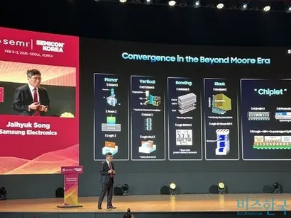
'cHBM·zHBM' Samsung's Co-Optimization Strategy
This year’s SEMICON Korea, hosted by SEMI (Semiconductor Equipment and Materials International), was held at COEX in Gangnam-gu, Seoul, with approximately 550 companies participating, making it the largest event to date.
Representing Samsung Electronics, CTO Song explained the company's 'co-optimization' strategy, leveraging its capability to handle everything from 'Design to Foundry and Memory.' Song emphasized, "Samsung's primary goal is to fully support customers amidst the explosive expansion of AI," and unveiled the direction for its next-generation product lines, cHBM and zHBM.
Regarding cHBM, Song elaborated, "We are considering a Samsung custom HBM where the base die handles certain tasks currently performed by the Graphics Processing Unit (GPU)." The idea is to have the base die—the core chip at the bottom of the memory—share the load of the GPU to maximize overall system efficiency.
He introduced zHBM as having four times the bandwidth and one-fourth the power consumption of HBM4. He highlighted that while conventional HBM is placed alongside computational units like CPUs or GPUs, zHBM can improve bandwidth and power efficiency by stacking DRAM directly onto the computational unit.
The next-generation technology roadmap also included a vision for interface innovation. The strategy is to strengthen research into optical technology that uses light to overcome the limitations of electrical signal-based connections and to apply NAND stacking know-how to DRAM to innovate its architecture. Song stated, "We will go beyond simply making good chips and respond to the demands of the AI era through fundamental changes in system structure."
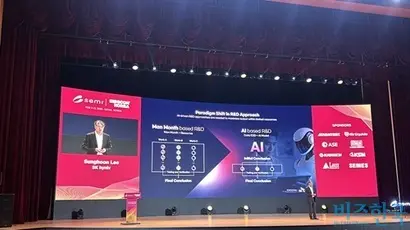
Emphasizing 'Tech Platforms' and AI-Driven R&D Transformation
SK Hynix Vice President Lee Sung-hoon highlighted the need for a 'tech platform' strategy and ecosystem cooperation to respond to increasing technological difficulty. He explained that while the company previously applied new technologies individually for every product development cycle, it has recently shifted to a platform concept, modularizing key processes to utilize them for two or more generations. This has minimized risks and development delays associated with generational shifts.
He also addressed the current demand for material innovation. With the miniaturization of semiconductors, it has become necessary to explore new channel materials, and he determined that it is difficult to maintain speed using only traditional, labor-centric development methods. As an alternative, he announced plans to move away from the human-centric approach and introduce an AI-based development system to maintain a 'development cadence' (development cycle). Lee noted, "While previous R&D relied on adding more personnel and resources, we must now actively incorporate AI."
However, he noted that there are limits if AI adoption remains at the individual company level. "The semiconductor industry is sensitive to IP and data protection, so data is not shared easily; however, the AI era requires data utilization and cooperation at the ecosystem level," he said. Given the nature of the industry where equipment, materials, and manufacturing are closely linked, it implies that data-driven optimization must occur across the entire supply chain.
Jeong So-young, CEO of NVIDIA Korea, who spoke on behalf of Timothy Costa, Director of Business Development at NVIDIA, said, "NVIDIA is evolving beyond a semiconductor company into an AI infrastructure company, and in this journey, South Korea is an incredibly important country in the overall semiconductor market."
She also emphasized the combination of physical AI and manufacturing sites. "Cooperation, such as modeling factory environments and training robot systems through NVIDIA's Omniverse-based simulation, is actively taking place across South Korean manufacturing," Jeong said. "We will go beyond being a simple player and act as an 'innovator' that leads new innovations based on AI factories alongside Korean companies." This reflects the trend of implementing and optimizing manufacturing processes in digital environments.
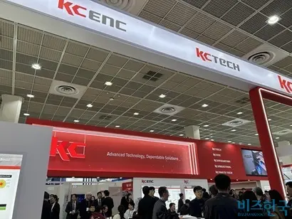
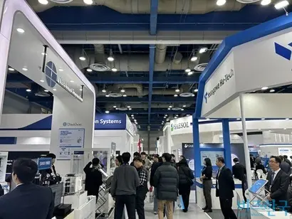
This year's SEMICON Korea set a record for the largest scale and number of participating companies. According to the organizer, the exhibition, which runs until the 13th, expanded its space to cover the entire COEX facility and nearby major hotels to accommodate demand. The domestic semiconductor ecosystem, centered on Samsung Electronics and SK Hynix and connecting design, manufacturing, equipment, materials, and parts, is considered a global competitive strength. The event confirmed the high interest in the Korean market and its ecosystem, especially as the strategic value of the semiconductor supply chain grows alongside rising AI demand.
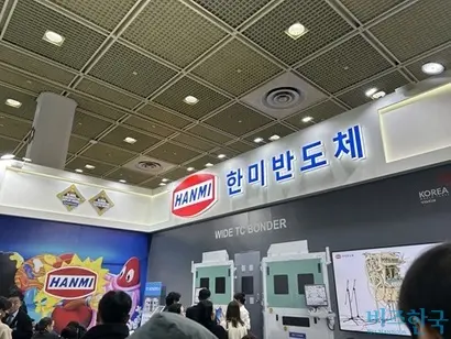
The exhibition hall featured booths from domestic firms such as Hanmi Semiconductor, Jusung Engineering, Wonik Corporation, GSTEM, and Shinsung E&G, alongside global equipment manufacturers including ASML, ASM, and Tokyo Electron (TEL).
Each company highlighted its cooperation with the three major memory makers: Samsung Electronics, SK Hynix, and Micron. Femtron showcased HBM inspection equipment, which analyzes the state of wafers and dies by performing 2D and 3D visual inspections simultaneously. A representative from Femtron said, "We precisely measure warping or tilt in dies and wafers that occur during the HBM stacking process and detect micro-defects through 2D/3D surface inspection. Our equipment is currently supplied to SK Hynix's Icheon and Cheongju sites, and we have already secured additional order schedules for this year."
GSTEM introduced environmental control technology within EFEM, which is semiconductor transport equipment. This technology prevents moisture in the atmosphere from causing surface defects and affecting yields. A GSTEM official explained, "We replace the air inside the wafer containers with nitrogen to create a low-humidity environment, preventing corrosion or defects. We are supplying products to the three global memory companies, including Micron, Samsung Electronics, and SK Hynix."