

[비즈한국] In the era of Artificial Intelligence (AI), the hottest topic in the semiconductor substrate sector is 'glass'. Glass substrates are considered ideal for AI semiconductors because they offer higher durability and power efficiency compared to the organic materials, such as plastics, used in existing semiconductor processes. Due to the nature of glass, which is vulnerable to external shock and pressure, it has previously been classified as 'over-spec' due to the difficulty of achieving high yields. However, with the rise of AI, it is drawing attention as a material that could shift the competitive landscape. As Samsung begins to enter the glass substrate business in earnest, the stock prices of related companies are fluctuating. Can these glass substrates, which have yet to even be commercialized, truly become a game changer?
The Industry Jumps In: 'Is Silicon Out and Glass In?'
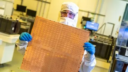
Glass substrates, which have emerged alongside the AI craze, are being called 'dream substrates.' When drilling holes to connect multiple semiconductors, using smooth glass—as opposed to plastic or silicon materials—can dramatically increase data processing speeds even with the same power consumption. This is because there is less degradation of electrical signals and less heat generation. They also have higher structural integrity than existing organic substrates, meaning they do not warp at high temperatures and are advantageous for manufacturing large-area substrates. Absolics, a subsidiary of SKC011790, expects power efficiency to improve by about 50% compared to existing organic material substrates.
This year is expected to be the inaugural year for verifying the technical reliability of glass substrates. The industry is also reorganizing its business structures and preparing for mass production. According to industry sources, Samsung Electronics005930 is seeking cooperation with group affiliates to apply glass substrates to its semiconductor mass production processes. The project is reportedly being led by the Foundry (consignment production) division of Samsung Electronics' DS (Semiconductor) unit.
Following Samsung Electro-Mechanics005930, which is building a pilot production line at its Sejong plant, it appears that Samsung Electronics will focus on competitive edge in advanced packaging services that even cover High Bandwidth Memory (HBM). Samsung Electro-Mechanics plans to go through customer sample promotions this year and target product mass production after 2027. Lim So-jung, a researcher at Yuanta Securities, explained, "As an IDM (Integrated Device Manufacturer), Samsung Electronics is focusing on the fact that by securing the glass substrate market, it can strengthen its overall corporate competitiveness through collaboration between its system semiconductor production area—foundry—and the TSP (Total Solution Provider) division responsible for post-processing."
SK, which is at the forefront, also has high expectations for glass substrates. After meeting with NVIDIA CEO Jensen Huang during CES 2025, SK Group Chairman Chey Tae-won held up a model of his company's glass substrate at the SK booth, stating, "I just sold some." Absolics is a company established in 2021 by SKC and the world’s largest semiconductor display equipment manufacturer, Applied Materials of the United States. Absolics has completed a glass substrate factory in Georgia, USA, and has set the target for product mass production for 2026.
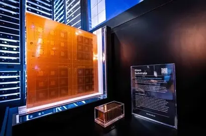
LG's development schedule is also underway. Moon Hyuk-soo, CEO of LG Innotek011070, also stated at this year's CES that "glass substrates are the direction we must move toward," and announced plans to begin prototype mass production by the end of this year. LG Innotek made its entry into the glass substrate business official in March of last year, and it is observed that they will begin trial production at their Gumi plant. As for Intel, it is accelerating progress by investing $1 billion in glass substrate research and development (R&D). It unveiled a prototype in September 2023 and plans to launch glass substrate-based CPUs and AI semiconductors by 2030.
Still 'Theoretical', Still a 'Long Way to Go' for Commercialization
Semiconductor substrate materials have changed in 15-to-20-year cycles. As organic substrates have been mainly used since 2000, the industry is at a turning point in terms of timing as well. Currently, silicon is the most widely used material for semiconductor substrates. While it has excellent durability and electronic control performance, it is weak against high voltage and high temperatures above 150°C. Although silicon interposers are used as a solution, the problem is their high cost. In the AI sector, which handles massive amounts of data, the limitations are clear. Conversely, glass substrates are resistant to heat and electricity. They have a smooth surface, which is advantageous for creating fine circuits, and because they do not require an intermediate substrate, they have the advantage of being able to reduce substrate thickness by approximately 25%.
The industry expects that once glass substrates are utilized in earnest, it will have the effect of advancing semiconductor micro-fabrication by more than two generations. An industry insider said, "SKC is focusing on packaging technology verification and securing yields, and major global companies such as Intel and Taiwan's TSMC are also preparing for commercialization, considering the importance of packaging."

Global market research firm The Insight Partners forecast that the global glass substrate market will grow at an average annual rate of about 5.9% from $23 million (approximately KRW 33.2 billion) last year, reaching $4.2 billion (approximately KRW 6.06 trillion) by 2034.
However, the reason why glass substrates, which have been researched for nearly 20 years, have not yet been commercialized is also clear. They are vulnerable to external shock or cumulative pressure, making it difficult to increase yields during manufacturing, and sales prices are inevitably high. The "dream substrate" is still closer to a new technology at the conceptual stage, and many obstacles are expected.
For this reason, experts believe that directionality and technological prowess are crucial for glass substrates to be commercialized. Ko Eui-young, an electrical and electronics researcher at Hi Investment & Securities, emphasized, "A reconfiguration of the supply chain and reliability verification related to glass materials are necessary. Standardization work for mass production must accompany it, but even with mass production, the yield remains uncertain." Technically, improvements are needed in △forming holes for electrical connections, △uniformly filling conductive materials, and △inter-layer circuit connections and precise processing.
Researcher Ko noted, "However, if companies can sell them at a sufficiently high price due to the strong demands of clients who want to create high-performance semiconductors through advanced packaging, the low yields can be compensated for," adding, "The directionality indicating that a new inflection point is approaching is noteworthy."